Free DFM Analysis made by 20+years experience engineer
We have many customers have good designs ,but also some designs are poor for us to manufature, it is not complex board but it is poor design. That is why we usually say "An engineer who does not understand PCB manufacturability design can not have a good PCB design".
PCB Design ≠ PCB Manufacturing
PCB design is theory,manufacturing is practical.So there is a DFM check before manufacturing. DFM is design for Manufacturing. In the electronics industry, the quality and reliability of products depend primarily on the manufacturer’s process capabilities. The PCB factory is not a black box production line. It’s not that you give them the relevant PCB design data, and you can get a finished product that is precisely the same as the PCB design after a few days.
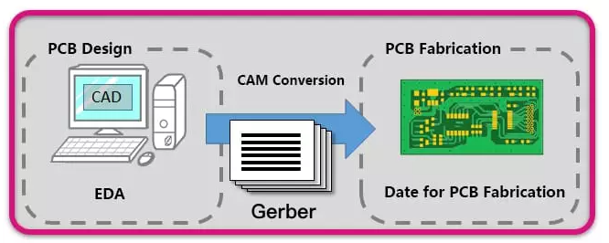
PCB design is a complete and rigorous process system, and PCB manufacturing is another set of sophisticated production and processing systems. At the same time, PCB design data is not equivalent to PCB manufacturing data. In other words, PCB manufacturing does not directly use PCB design data. PCB design data needs to be converted into production data for machines through CAM (Computer-Aided Manufacturing).In PCB factory, there are MI engineers to make instructions for each jobs ,and CAM engineers to do CAM work---change gerber file to working file in CAM software.

PCB Designers Need to Understand the PCB Manufacturing Process
Suppose the PCB designer does not understand the PCB manufacturing process and the CAM data conversion process, or the CAM engineer does not understand the relevant terminology of PCB design. In these cases, there will be problems in the data conversion from PCB design to PCB manufacturing.
Especially for “low-level” format files, like Gerber, that describe a single image, you also need an additional description file to describe your PCB manufacturing requirements, such as impedance control, layered structure, surface finish, and so on.
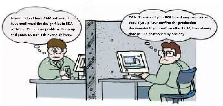
The information used for PCB manufacturing can be placed in an additional Gerber file, or it can be placed in a document file like Word for description in graphic form. However, where there is a text description, there will be problems with expressing and understanding the information; it is necessary to use telephone, email, or other communication tools to communicate and confirm. Suppose both parties use their professional terms to describe the problem and cannot clearly understand it. In that case, they all think that the other party does not know everything, and low-efficiency or even wrong communication is often the culprit for PCB manufacturing failures.

Why PCB Manufacturability Inspection and Analysis?
As a qualified and excellent PCB designer, a designer/engineer will try his best to avoid leaving the problem to the PCB manufacturer. Before submitting the manufacturing data, the PCB designer should check it in the CAM. He needs to check the design from the perspective of the PCB manufacturer during layout and adjust the PCB Layout design according to the process capabilities of different PCB manufacturers. This process is DFM (Design For Manufacturing). It requires us to understand the manufacturing process, production process, board performance, etc., of the cooperating PCB factory while designing the PCB.
You might think, why do you want to layout from the perspective of a PCB board manufacturer? It is not to increase the workload for ourselves, nor reduce the workload of the CAM engineers of PCB manufacturers. It is because we want the printed circuit boards produced by PCB factories to be qualified products. Suppose the product is defective due to errors in the design documents or manufacturing information. In that case, the final impact will delay the progress of our project, and we will still suffer the loss.
It Would Be Best If You Had a Helpful PCB CAM Engineer with over 20+ years
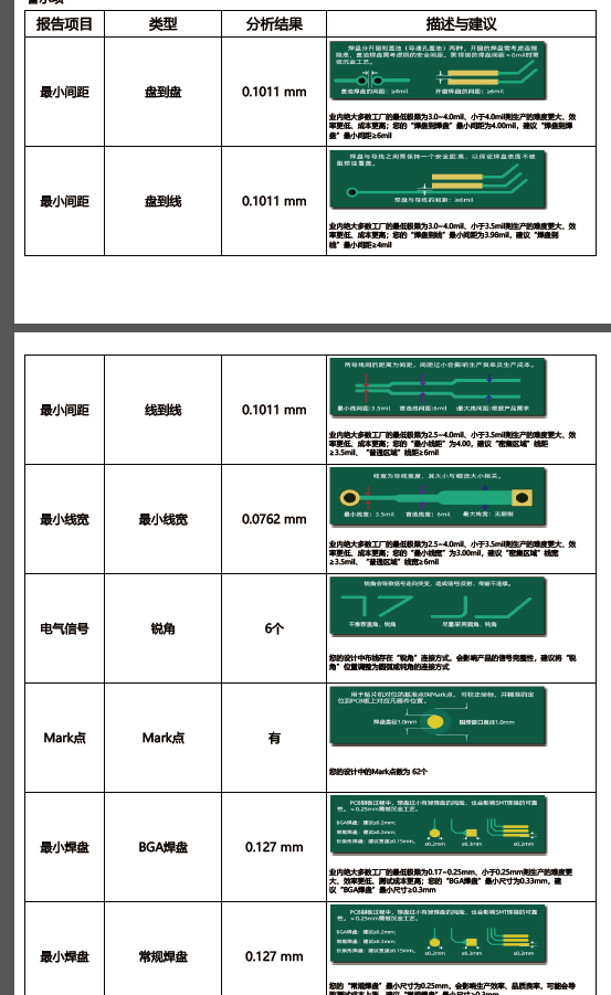
Our engineering manager have 20+ yeas in PCB.We can check your PCB gerber file or design file in 10-30 mins and feedback to you if there are any issues to produce. We have free DFM reports for any PCB files.

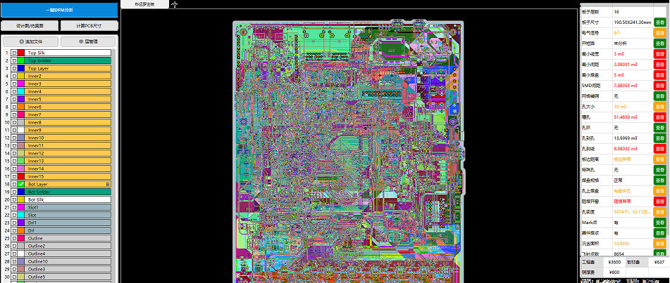
16 layers PCB DFM report
