-

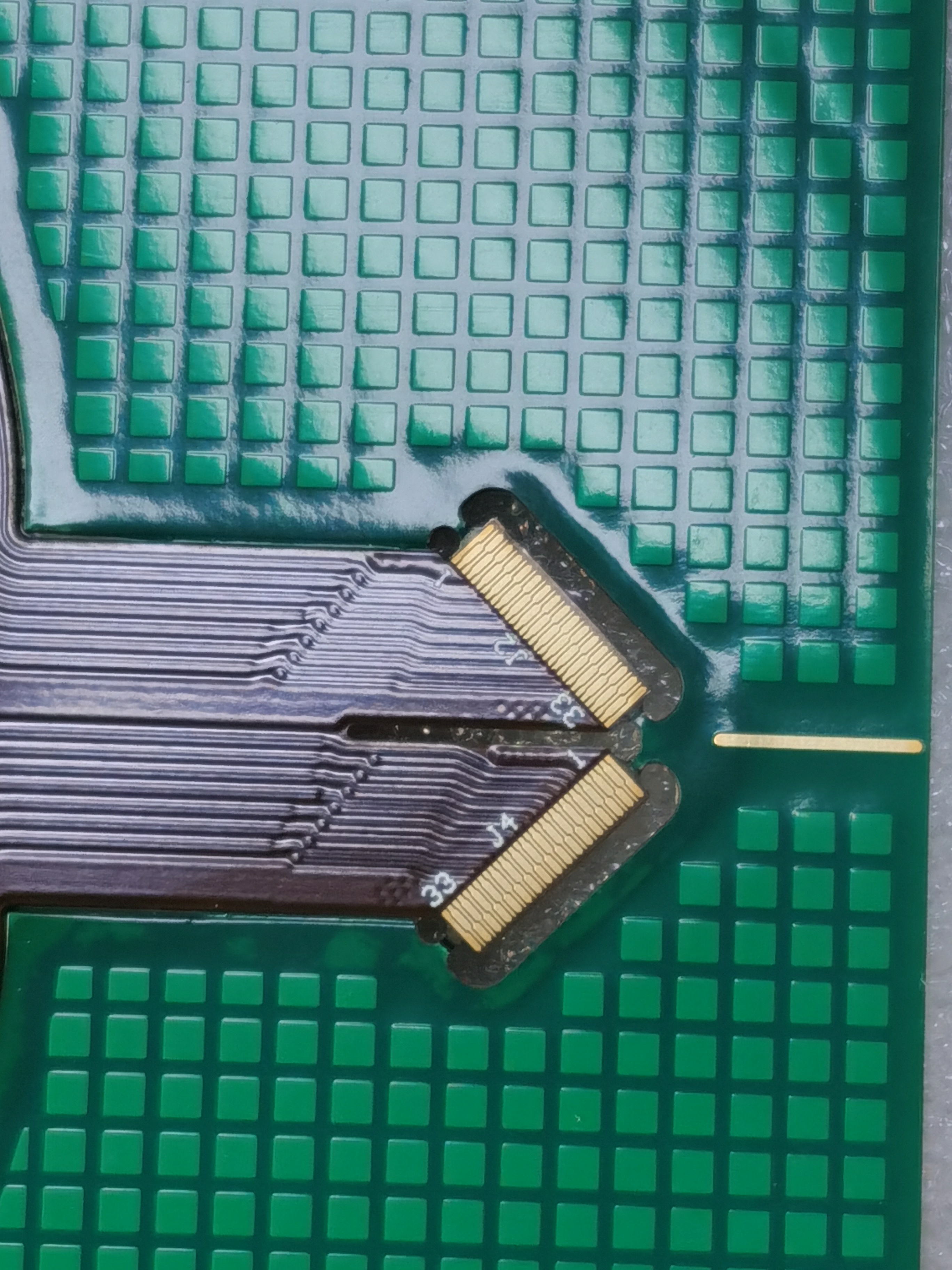
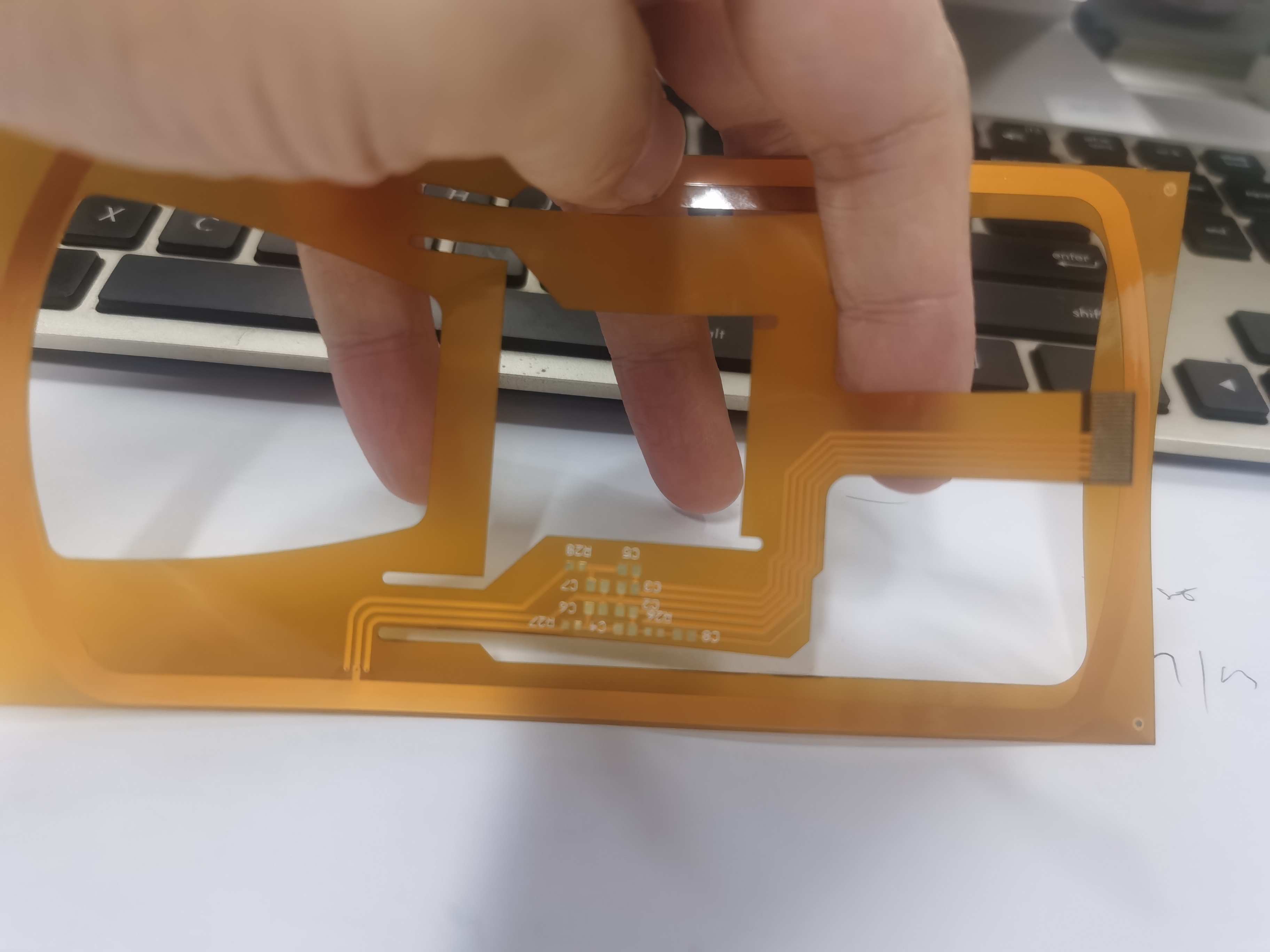
4 layer rigid-flex PCB with HDI design
¥ 0.00Buy now
-

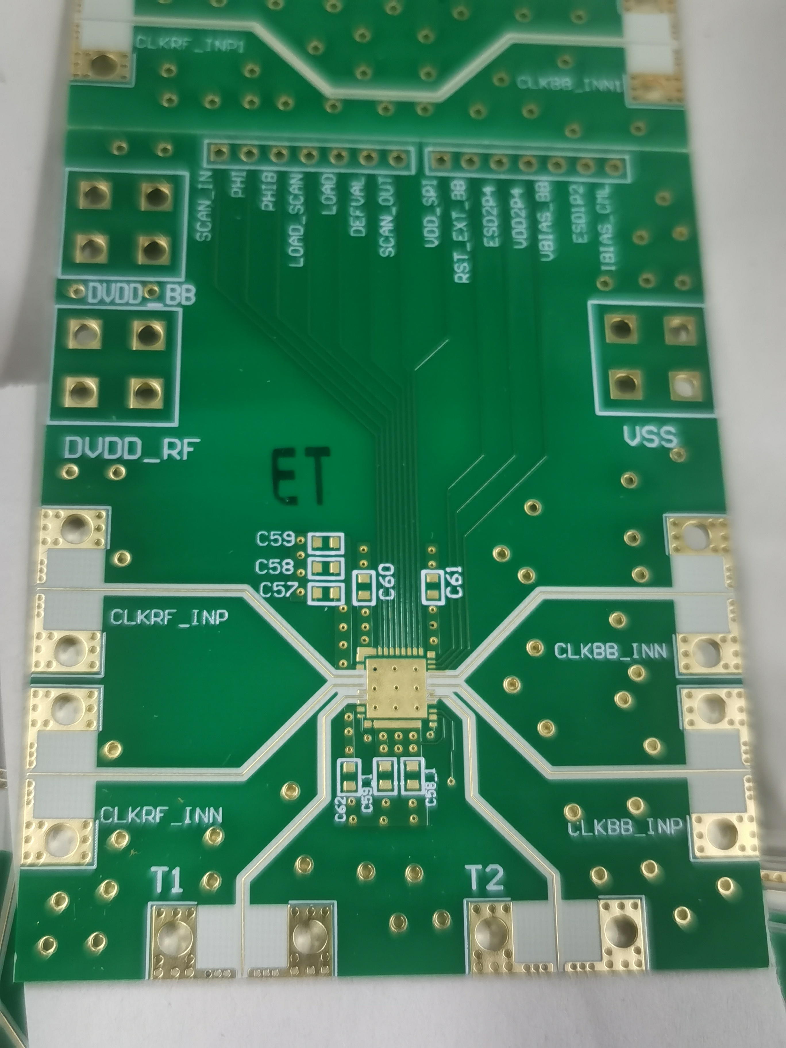
12 Layer Rogers PCB with blind vias L1-L2,L1-L6
12 Layer Rogers PCB
Blind Vias:L1-L2 ,L1-L6 ,
via in pad /POFV (Plated over filled vias)
Thickness:2.6mm Full gold at bottom side
Blue solder mask, White silkscreen¥ 0.00Buy now
-

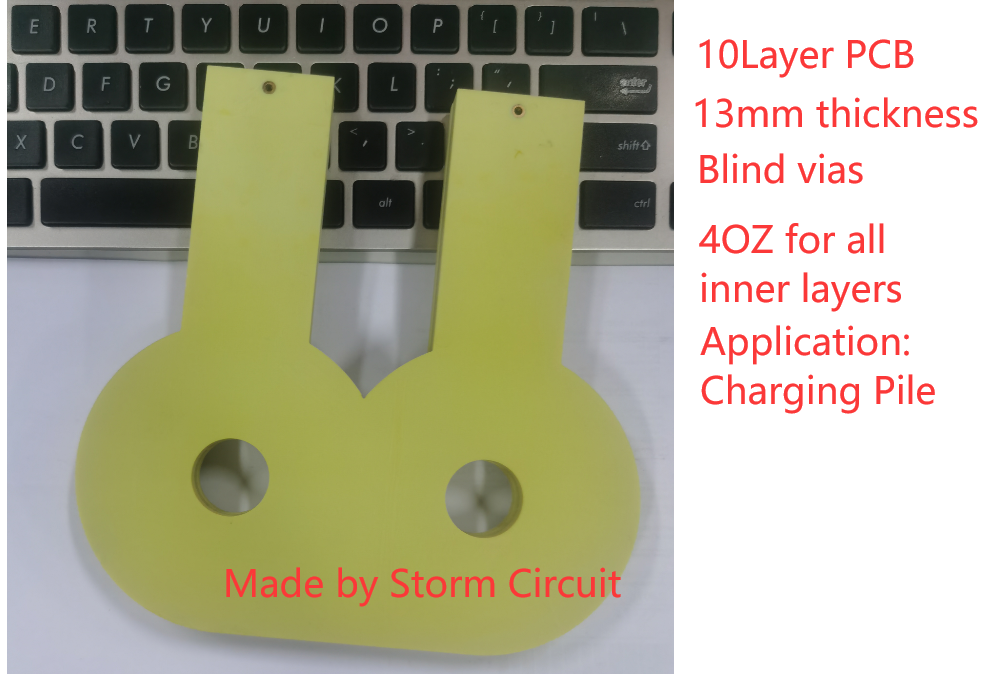
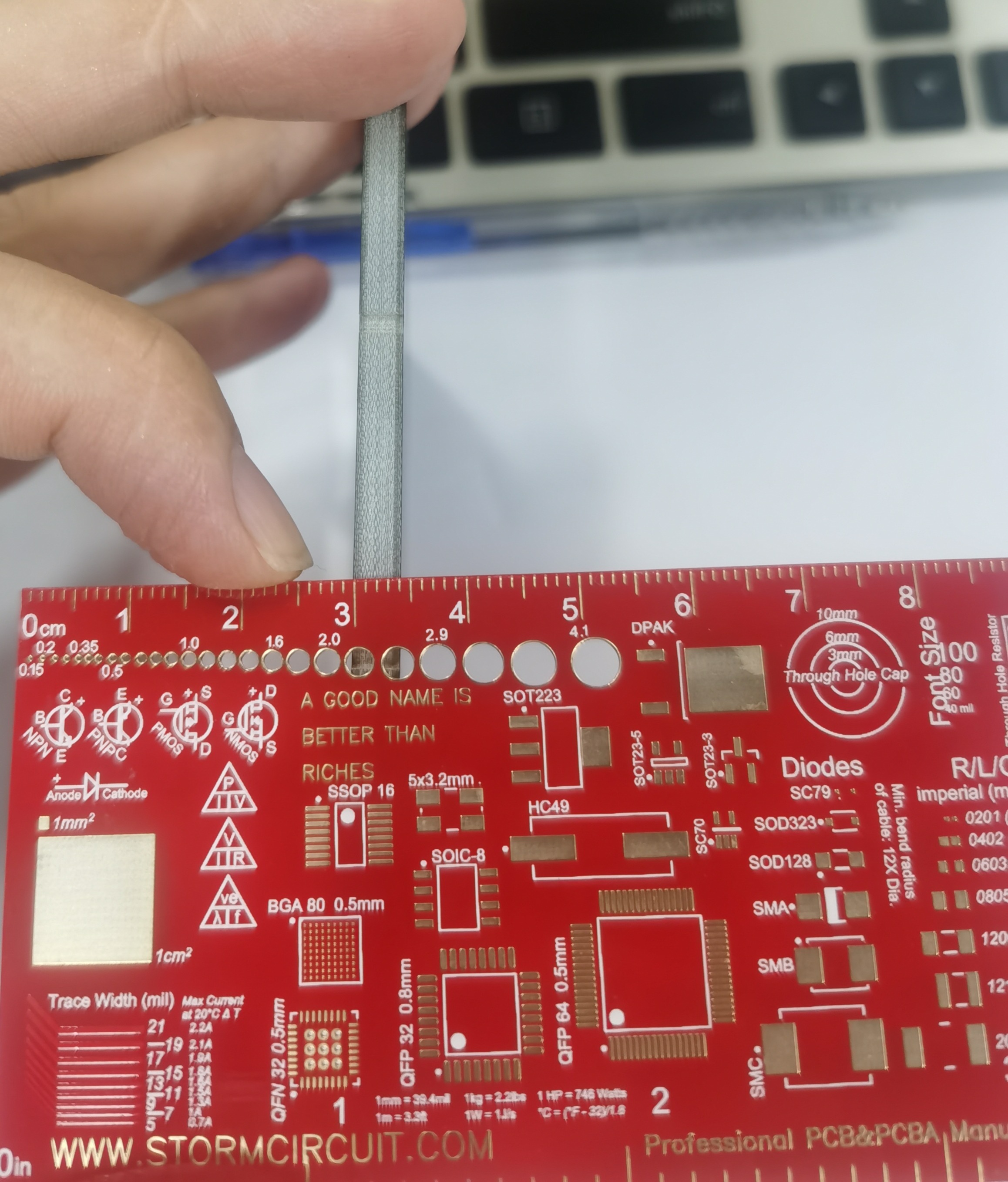
10 Layer PCB with 13mm
10 Layer PCB with 13mm
4OZ for all inner layers
Buried vias from L2-L9
dielectric thickness is 5mm between L1/L2 and L9/L10¥ 0.00Buy now
-

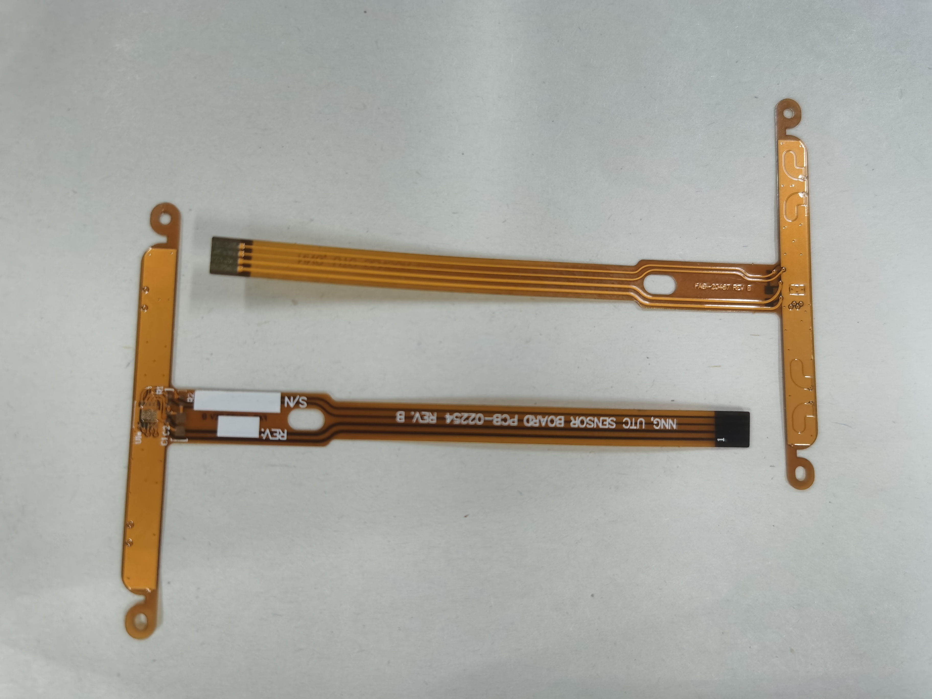
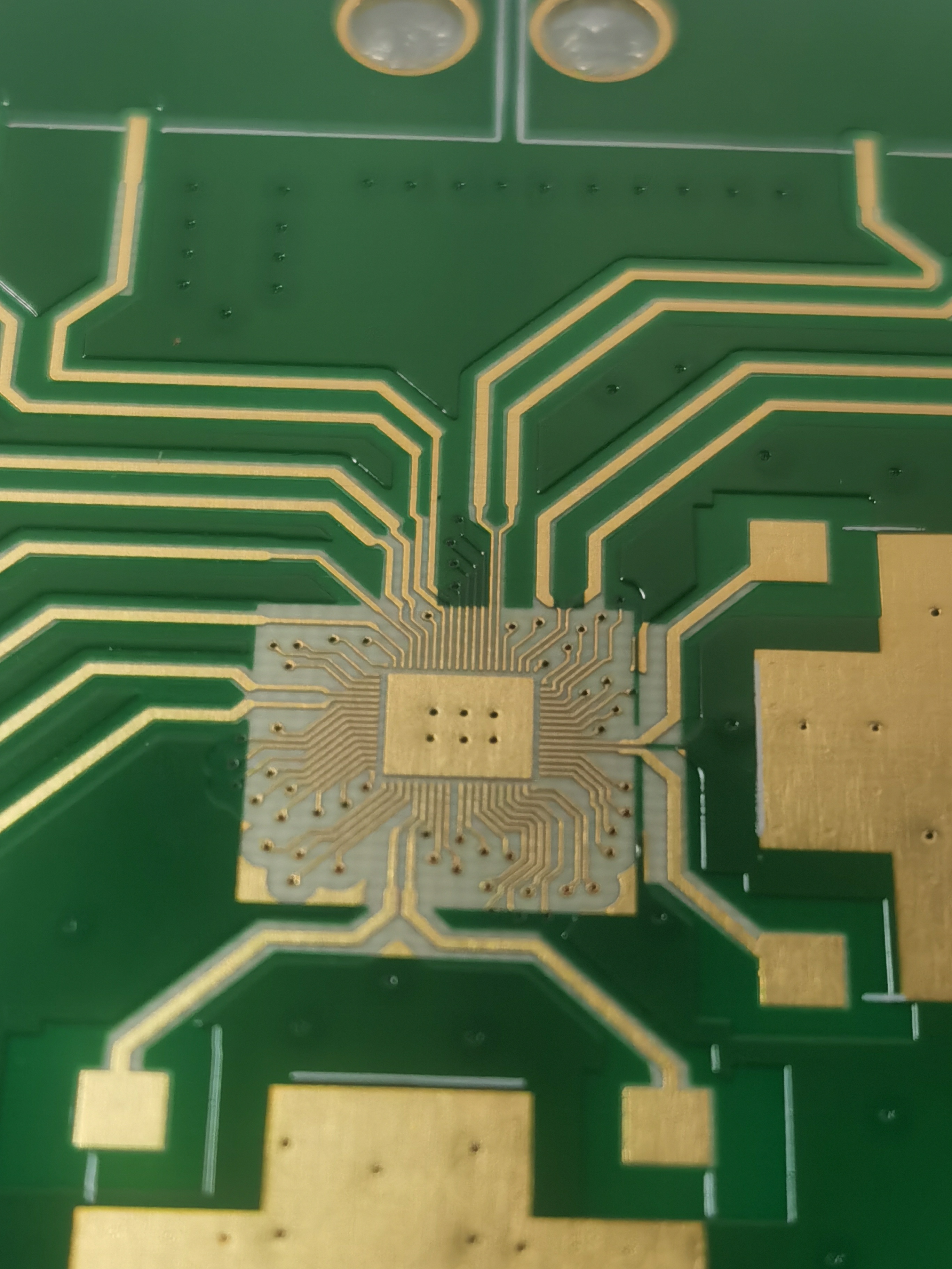
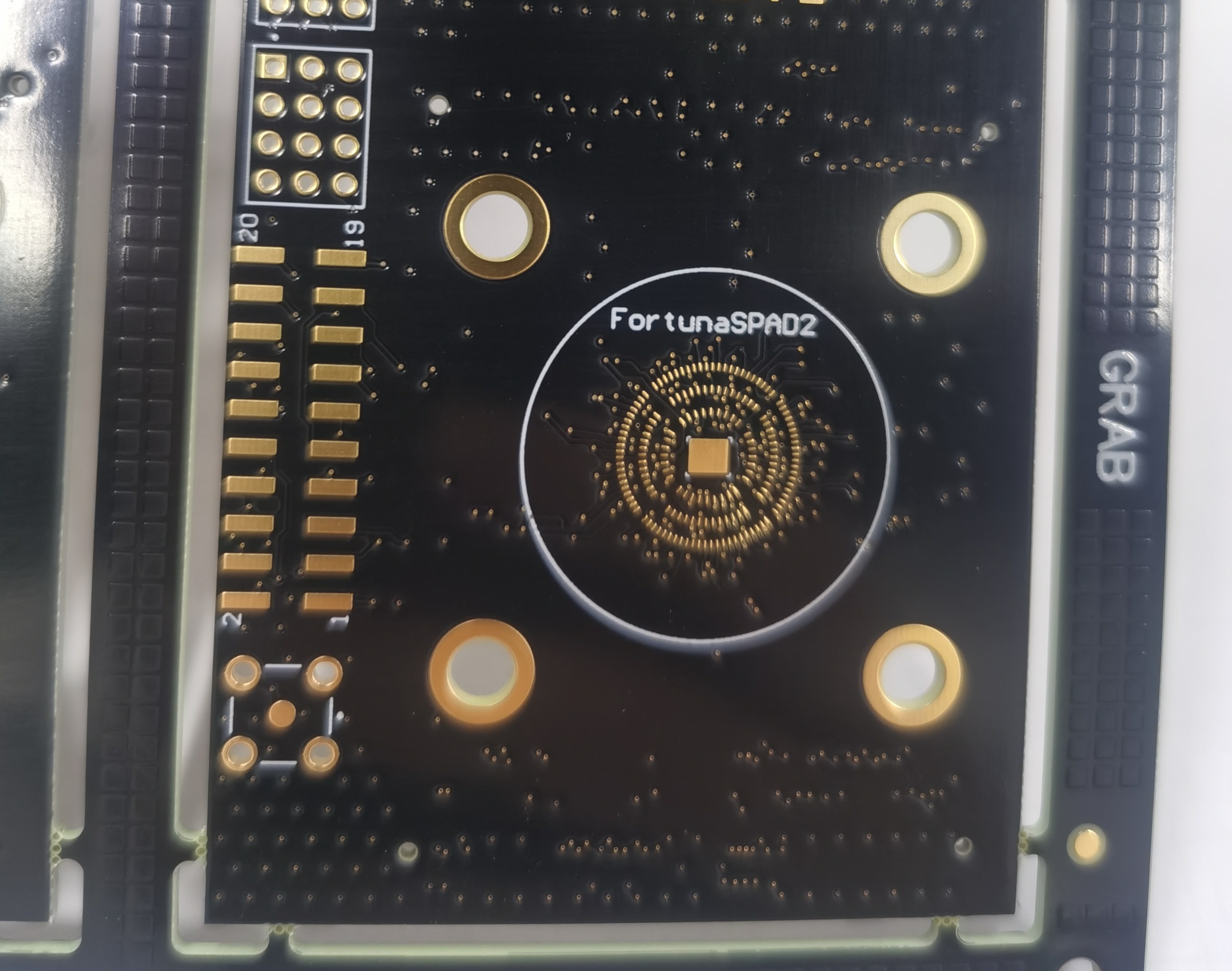
4 Layer HDI PCB with 0.38mm pitch BGA
4 Layer HDI PCB with 0.38mm pitch BGA
Min hole:0.15mm
Min trace/space: 0.076/0.0/76mm
0.38CSP
Blind Vias:L1-L2
Via in pad, POFV (Plated over filled vias)
4 layer 1.0mm Laser drilling¥ 0.00Buy now
-

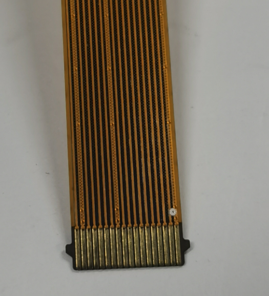
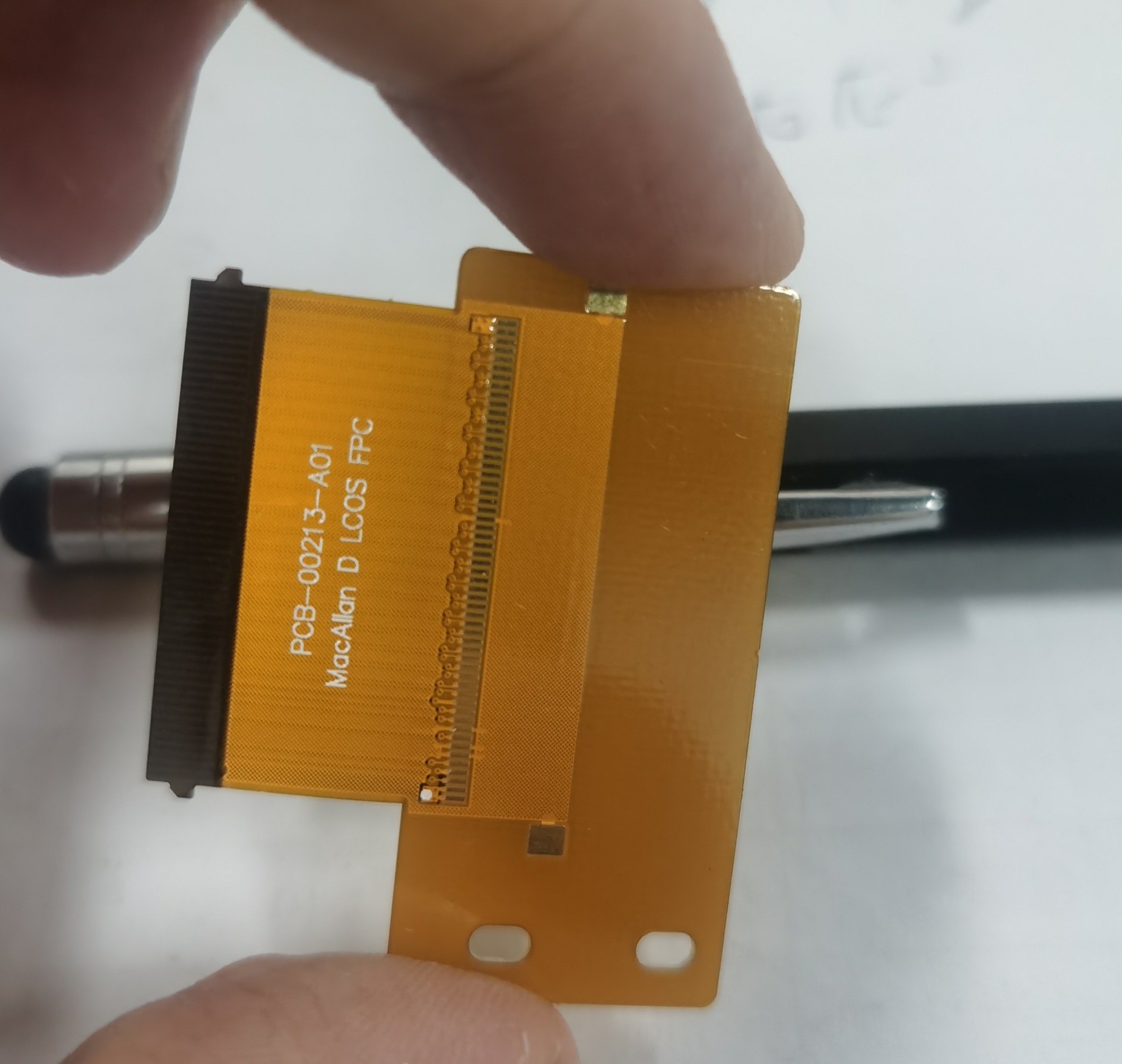
2 Layer FPC with hard gold plating 30U''
2 Layer FPC with hard gold plating 30U''¥ 0.00Buy now
-

Quick Turn HDI PCB--shipping in 5 days
Two designs,4 layer HDI PCB,0.4mm pitch BGA¥ 0.00Buy now
-

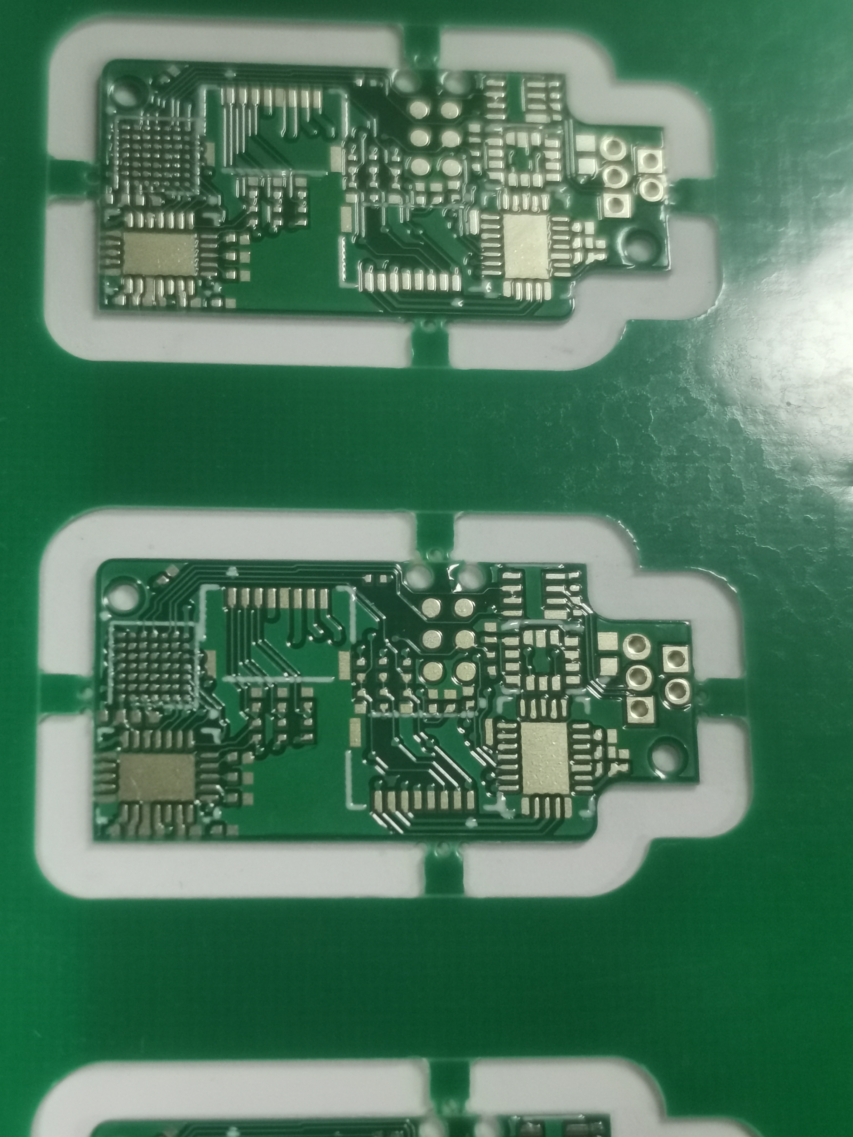
4 layer HDI with 0.4mm,shipping in 5 days.
4 layer HDI
HDI:L1-L2,L1-L3,
Via in pad
Half hole plating
Quick Turn shipping in 5 days.¥ 0.00Buy now
-

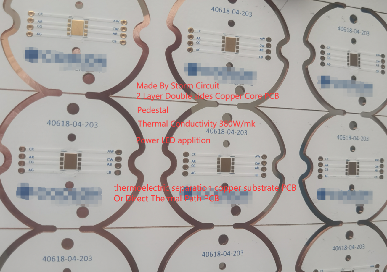
Thermoelectric separation copper substrate PCB---highest thermal conductivity with 380W/mk
2 layer double sided copper core PCB
ENIG
White solder mask, Blue silkscreen.¥ 0.00Buy now
-

2 layer FPC with quick turn in 3 days
0.2mm
Flex PCB
Stiffener with 0.3mm thickness¥ 0.00Buy now
-

ENEPIG for RO4350B with blind vias from L1-L2,L3-L4
ENEPIG for RO4350B with blind vias from L1-L2,L3-L4¥ 0.00Buy now
-

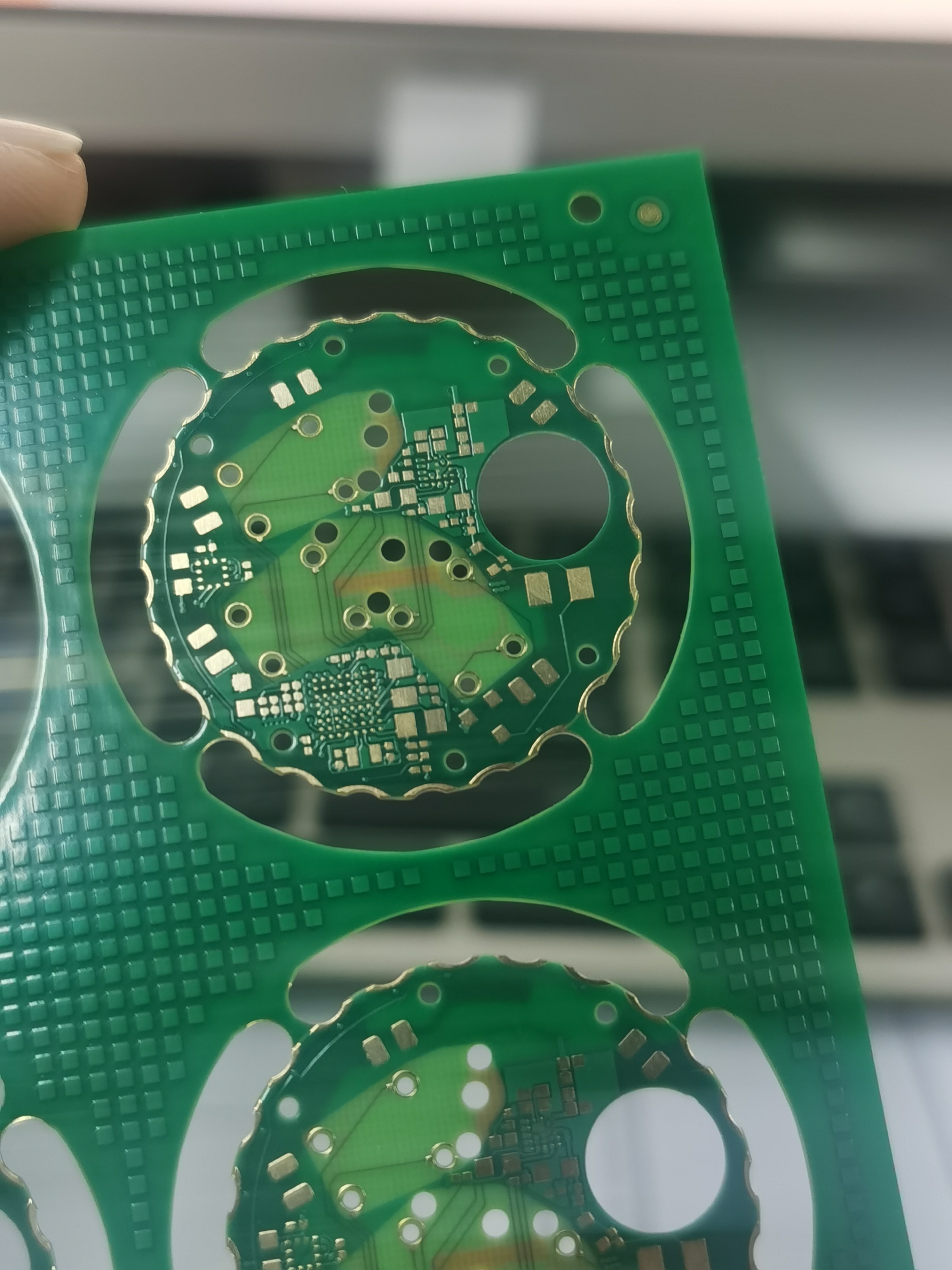
4.4mm PCB with blind vias and countersink holes
4.4mm PCB ,4 Layer
Blind vias L1-L2 ,L3-L4
Countersink holes
Matt Black solder mask
Via in pad
12:1 (Thickness :min hole)¥ 0.00Buy now
-

4 layer Flex PCB with 0.25mm thickness
4 layer
Flexible PCB
0.25mm
Stiffener¥ 0.00Buy now
-

4 layer RO4350B PCB with blind and ENEPIG
4 layer PCB
Material:All is RO4350B,6.6mil
Thickness:0.7mm
Surface: ENEPIG
Blind vias L1-L2,L3-L4
Min trace/space:4/4mil¥ 0.00Buy now
-

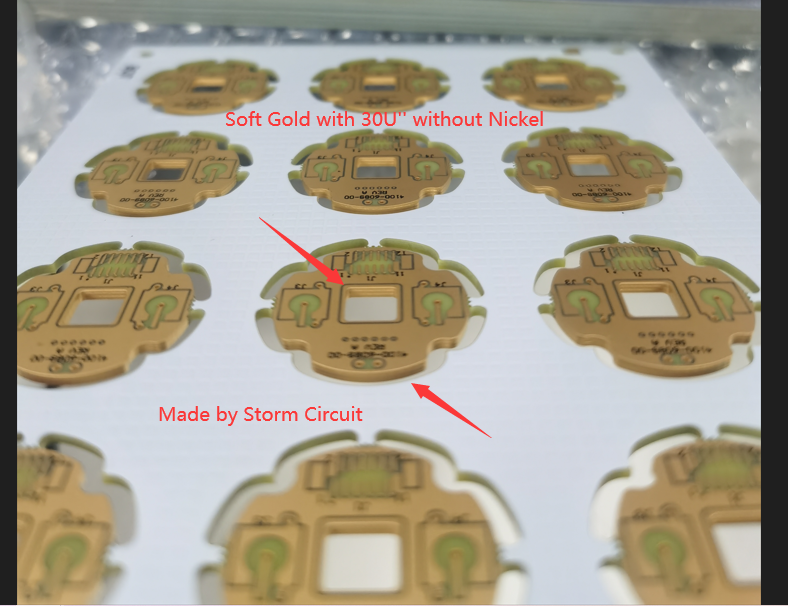
Soft Gold plating with 30 Micro inch PCB
FR4 :4 layer 1.6mm 1oz
Full gold at top and bottom side in units
Soft Gold with 30 micro inch
Edge plating
Black solder mask,white silkscreen¥ 0.00Buy now
-

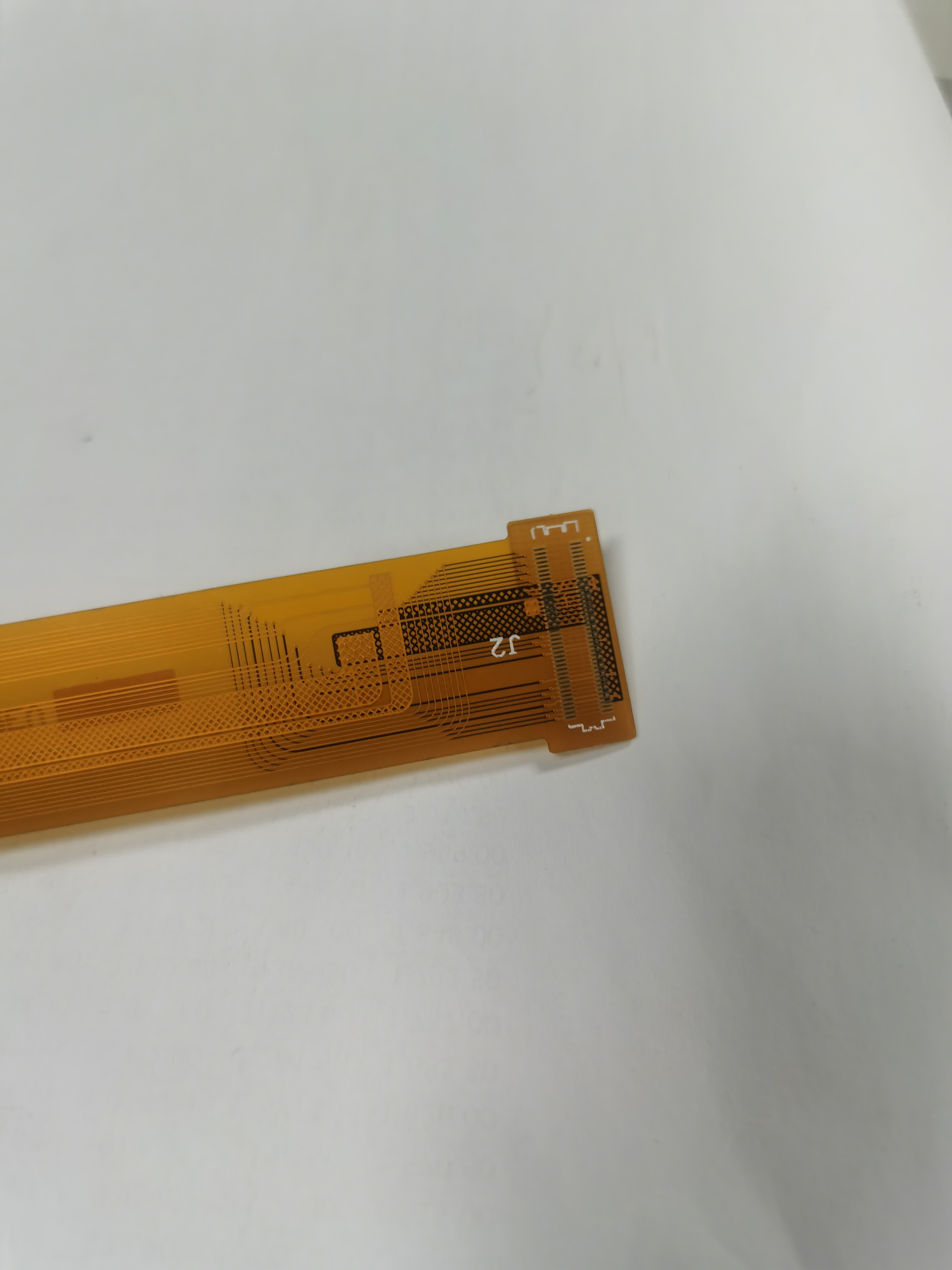
2 Layer FPC with 0.1/0.1mm gold fingers
2 Layer FPC
Thickness 0.2mm
min trace/space 0.1/0.1mm
FR4 stiffener total thickness 0.8mm
Storm Circuit loaded components too¥ 0.00Buy now
-

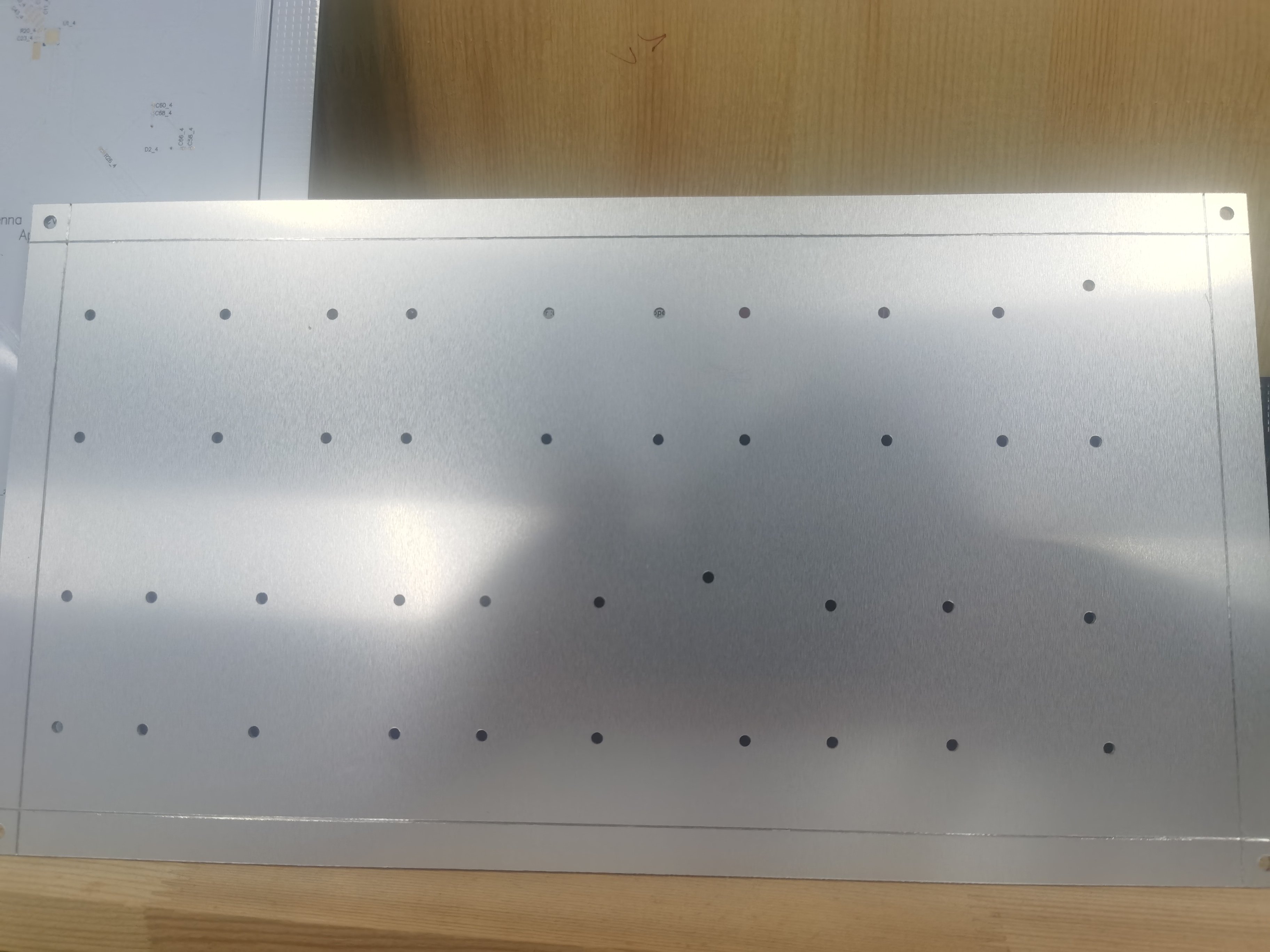
Sinlge layer Aluminum PCB
Sinlge layer Aluminum PCB--Metal Core PCB
Thickness 1.6mm
Black solder mask
White silkscreen
ENIG
Thermal conductivity:1.0W/mk¥ 0.00Buy now
-

4 layer PCB with 3.0mm thickness and 2oz copper
4 layer PCB TG170
Thickness:3.0mm
Copper : all layer is 2OZ
Blue solder mask
White silkscreen¥ 0.00Buy now
-

0.4mm pitch BGA PCB with 0.1/0.1mm
0.4mm pitch BGA
BGA pad 0.2mm
4 layer 1.6mm
min trace/space 0.1/0.1mm¥ 0.00Buy now
-

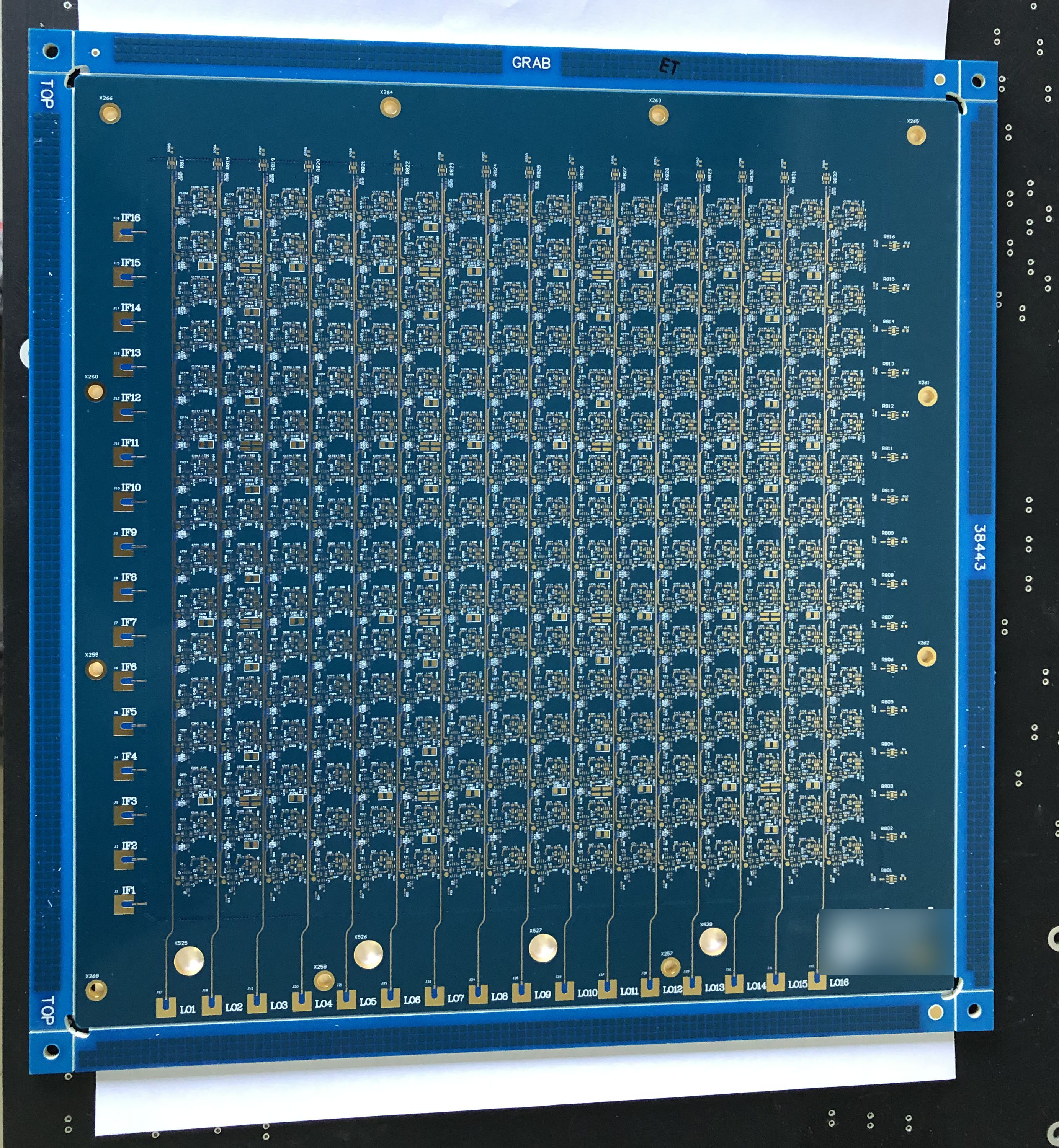
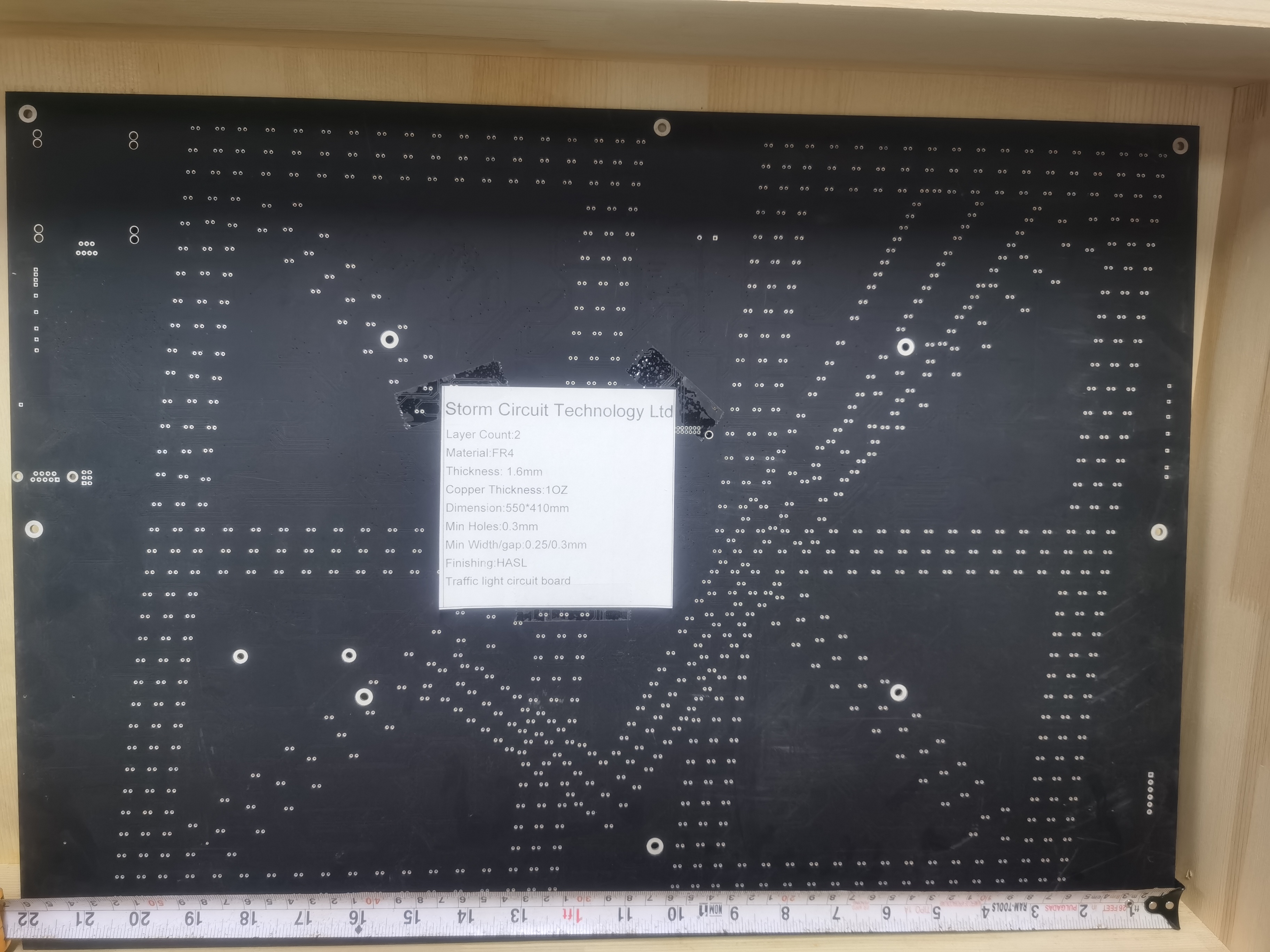
550*410mm large PCB
550*410mm large PCB
Thickness 1.6mm
HAL
Application:Traffic LED circuit boards¥ 0.00Buy now
-

4 layer PCB with RO4350B +FR4 designed by Columbia University
RO4350B +FR4
0.34mm RO4350B +PP+FR4
Impedance
Two designs
V-score
Immersion Gold¥ 0.00Buy now
-

8 Layer PCB with ENEPIG
8 Layer PCB
ENEPIG
1.6mm TG170
trace/space 0.1/0.1mm
min hole 0.15mm¥ 0.00Buy now
-

2 layer Flexible PCB with 1.0mm stiffener
2 layer Flexible PCB
Quick turn in 3 days
FR4 1.0mm +PI stiffener
Gold fingers
Impedance
trace/space 0.1/0.1mm¥ 0.00Buy now
-

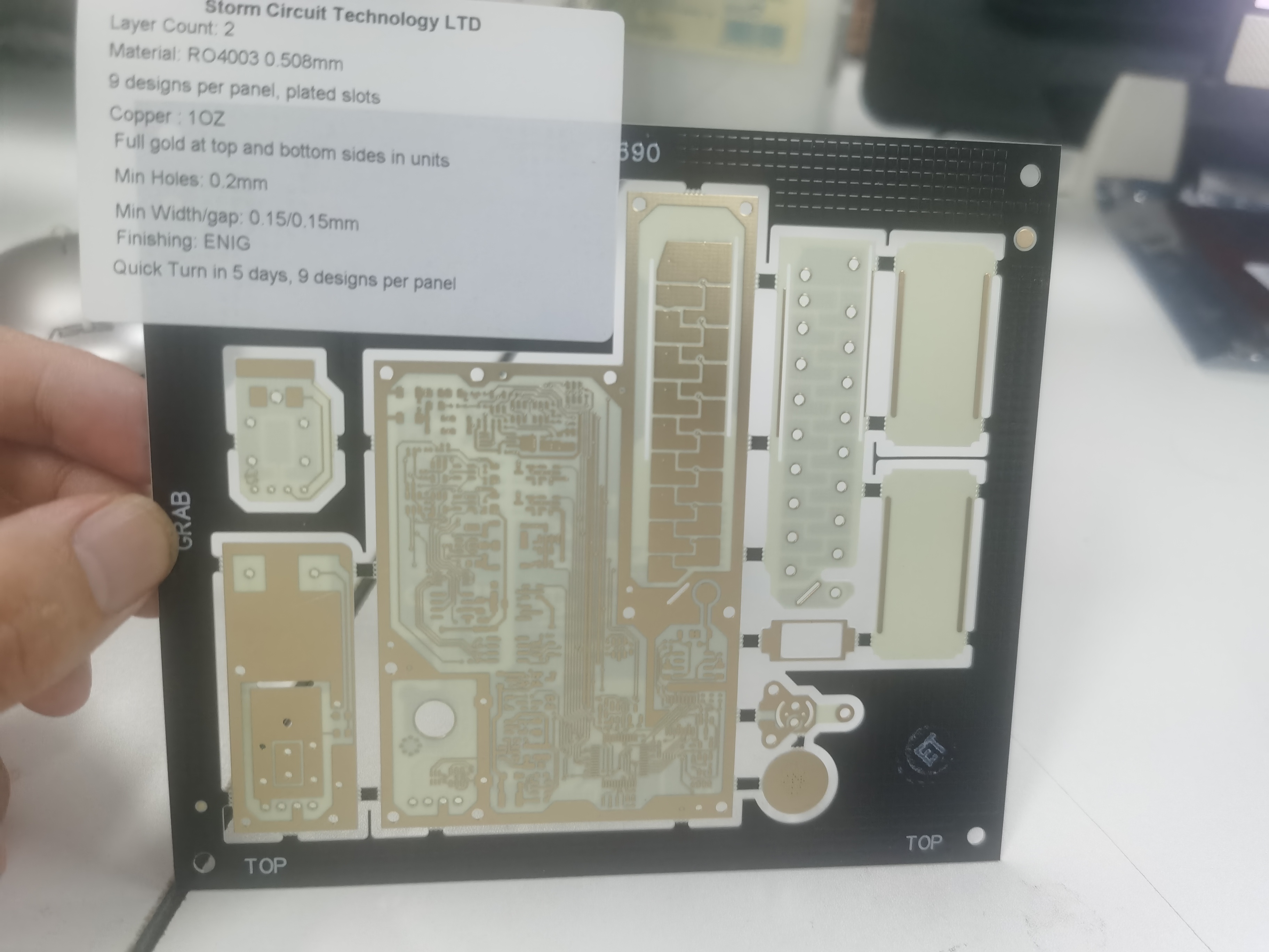
RO4003 0.508mm material
RO4003 0.508mm material ,
9 designs per panel,
plated slots.¥ 0.00Buy now
-

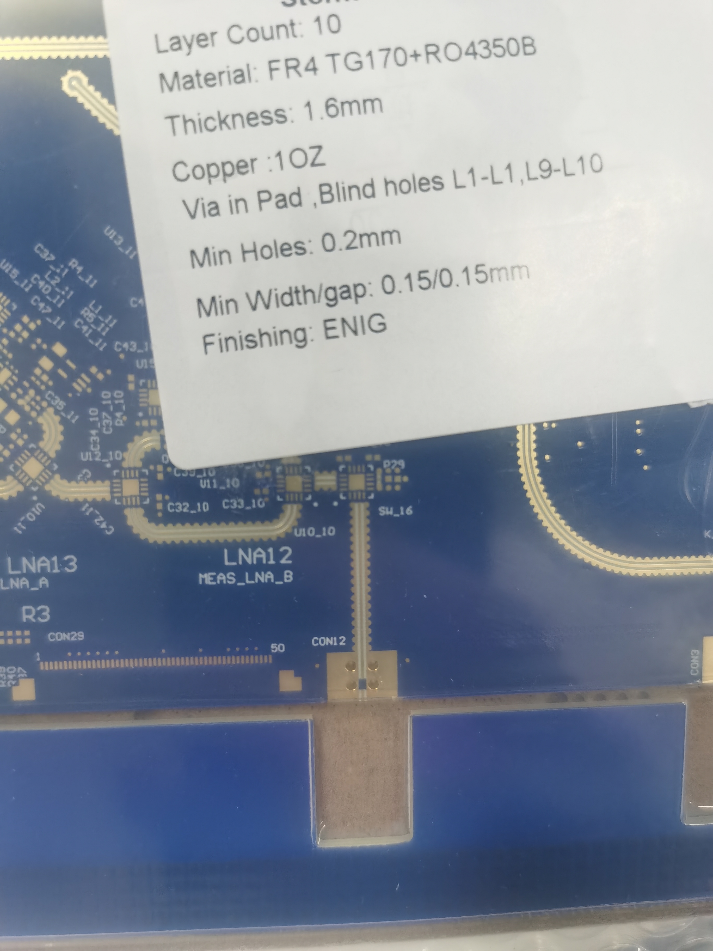
10 layer RF PCB with RO4350B+FR4
10 layer RF PCB with RO4350B+FR4
Blind vias L1-L2,L9-L10
Via in pad ,POFV
RO4350B 6.6mil¥ 0.00Buy now
PCB Products
Most are multi-layers board.Aluminum board---the base material is aluminum ,most used in LED,it requires high thermal conductivity.
PCB manufacturing process is very complex ,there are over 30 steps ,we will show you a very simple process here.
Double sided PCB:
Cutting Material-->Drilling holes--->Plating holes--->Outer layer
-->Etching-->Solder mask-->Silkscreen-->HAL(Gold)-->CNC (routing,v-cut)-->Testing-->Final inspection
Multilayer PCB:
Cutting Material-->Inner layer-->Press (stackup)--->Drilling holes-->Plating--->Outer layer -->Etching-->Solder mask-->Silkscreen--->HAL(Gold)-->CNC (routing,v-cut)-->Testing-->Final inspection
Storm Circuit offers a full range of PCB fabrication. HDI PCB , RF PCB ,Rigid-flex PCB ,ENEPIG PCB ,large PCB ,impedance control, via in pad, blind/buried PCB .etc
Full range of RF PCB / Microwave PCB and High Frequency materials /Rogers material in stock
10 years aerospace PCB manufacturing experiences
7/24 Live sales &tech support
24 hours fast prototype expedite services
4 Layers HDI PCB as quick as in 5 working days
10 Layer HDI PCB as quick as in 8 working days
16 Layer HDI PCB as quick as in 10 working days
4 & 6 & 8 Layer rigid-flex PCB made from 6 days to 12 days
Storm Circuit Technology Ltd, Made in China with Love.
2009-2022
