Brief introduction for Backdrilling Technology
PCB Backdrilling Technology
Backdrilling technology used in the semiconductor industry that ensures the highest fidelity signals can be carried at ever increasing speeds. This will ensure signal stubs are minimized; Stubs are the source of impedance discontinuities and signal reflections which become more critical as data rates increase. It is a preferred method in HS designs.
The advantages of the back drill via:
- Reduce noise interference
- Improve signal integrity
Reduce the use of buried blind holes, reduce the difficulty of PCB manufacturing that is the role of the back drill.
The purpose of the back drill is to drill through a hole that does not have any connection or transmission to avoid reflection, scattering, delay of high-speed signal transmission. It is shown that the main factors that affect signal integrity of the signal system are that vias have a great influence on the signal integrity except for design, board material, transmission line, connector, chip package and so on.
The principle of back drill production working
When the drill bit is drilled, the drill tip touches the copper foil of the substrate board generates micro-current to sense the height of the board surface, and then drill down according to the set drilling depth. It will stop when reach drilling depth.
The process of back drill
1,Providing PCB with a tooling hole, and make the drilling process.
2,Plating the hole before dry film sealing treatment.
3,Make outer graphics after the plating process.
4,Performing pattern plating on the PCB after forming the outer pattern, and performing dry film sealing treatment of ,the positioning hole before pattern plating.
5,Drilling the tooling hole and then drill back vias on need
6,Remove the residual after drilling back vias and cleaning them.
What the features of back drill via PCB?
- Most of the back drill are rigid PCB
- The layer is generally 8 to 50 layer
- Thickness:2.5mm or more
- Large PCB aspect ratio
- Large board dimension
- The outer layer is less trace, mostly for the press-fit holes square array design
- Back drill via is usually larger 0.2mm than vias that need to be drilled
- Back drill depth tolerance:+/- 0.05mm
- The minimum insulation thickness is 0.17mm
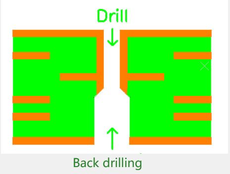
In PCB manufacture process, back drilling is 2nd drill operation that removes the unused plating in vias from a certain side to a certain depth.
Backdrilling prototype board
The major fabrication points of back drilling:
- Use new drill tool to reduce chip load.
- Check fabrication capability of the depth of back drilling.
- Control precision of drilling.
Storm Circuit offers a lot of HDI and Backdrilling PCBs.If you have any PCB questions,please do not hesitate to contact us.Hope we can help you in PCB solutions.