What is Blind Via PCB and why use blind vias?
Blind Via PCB is one of the most common printed circuit boards used in various modern electronic devices today, such as smartphones, laptops, touchscreen devices, game consoles, and many others. This is the PCB type that allows you to add multiple layers for the board and add higher density circuitries between the components on the board. This guide will provide you with useful information about the Blind Via PCB and how it works.
What is Blind Via PCB?
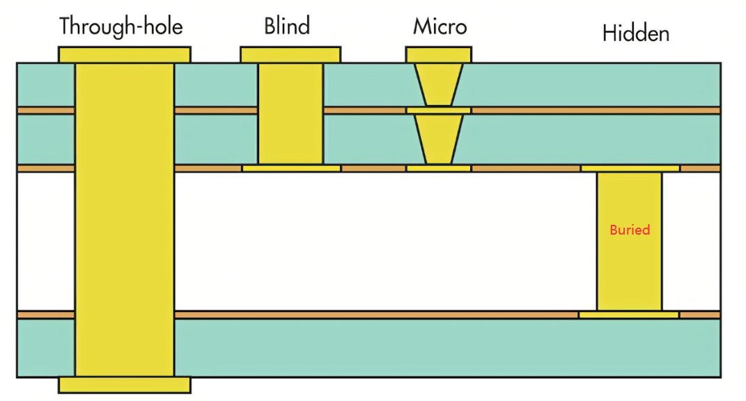
Blind Via PCB or HDI PCB is the type of circuit board which uses blind vias and other types of vias in its connection system to provide the high-density interconnection between different layers on the circuit board. The Blind Via PCB uses blind vias to connect the board surface to the inner layers of the board using hidden circuitries. Please note that the connection made with blind vias doesn’t go through the entire board.
Blind Via PCB often uses various microvia types, such as blind vias, buried vias, and the through-hole vias to connect multiple layers of the board together. The blind via will connect the outer layer of the board to the inner layers through the buried via inside the inner layers, and then the buried via will connect to the through-hole via, which is the microvia type that goes through all the layers of the board. This is the system that allows you to fit various components on a smaller board, since you will only need to add additional layers to your board and connect all layers on the board together with various microvia types.
Characteristics of the Blind Via PCB
The Blind Via PCB has a significant difference when compared to the regular PCB type, and it has various characteristics that make it unique when compared to other types of printed circuit boards. For instance, the Blind Via PCB uses multiple layers on a single board, which makes it unique when compared to the regular PCB that uses only a single board with no layering. Here are the characteristics of the Blind Via PCB:
- It uses different via combinations, such as blind via, buried via, and through-hole via. The reason is that the blind via cannot work without incorporating the buried via and the through-hole via for its connection. The blind via needs to connect to the buried via and the through-hole via, so that it can connect the multiple layers of the board together.
- The Blind Via PCB or HDI board has multiple layers. It uses the under-layer connection system that allows the board to connect multiple layers into one interconnected circuitry. This way, you can combine various components on a single board using the layering process, instead of using multiple boards to achieve the same result.
- It connects the components from different layers through the under-layer connections. Blind vias only connect the components using the under-layer connections. Only the upper side of the via is visible from the board surface. The remaining connection of the blind vias exists within the inner layers on the circuit board.
Blind Via vs. Buried Via – What are the Differences?
The blind via printed circuit board uses the blind vias and buried vias on a single board. These vias work together to create the under-layer connections that will interconnect with all layers on the primary board. However, blind via and buried via have their differences. Here are the differences between blind via and buried via:
- Blind via is visible from the board surface, while buried via doesn’t. Blind via is there to start the connection between the outer layer to the inner layers in the Blind Via PCB. Meanwhile, the buried via will become the in-between connector between the blind via and the through-hole via to interconnect all the connections throughout the board layers. Thus, the buried via will not be visible from the board surface.
- You will place the buried via in the middle of the connection between the blind via and the through-hole via. Buried via is a necessary connection point for the Blind Via PCB, and it will get placed inside the inner layers as the connection point for the multiple layers on the blind via board. Blind via can’t connect to the through-hole via without using the buried via in the middle.
- Buried via can help free up space for the outer layer of the board. You can use buried via to interconnect the inner layers of the Blind Via PCB while freeing up space for the outer layer of the board. The reason is that you can only place the buried via in the inner layers of the circuit board.
The Reasons to Use the Blind Via PCB for Your Projects
With the interconnected circuitry in the blind via circuit board, you can get various advantages when you use this board for your project. For instance, Blind Via PCBs can provide you with much more freedom in your board design, as you can stack multiple layers into one board. With the multiple-layer stacks, you can also fit many more components into a single board, which can help you save some space in building the interconnected circuits for your device. Here are some reasons to use the Blind Via PCB for your projects:
- You can fit various connections into one board while keeping a small form factor for the board. With the interconnected layer system in the Blind Via PCB, you can fit various connections into one board without having to worry about running out of space on the board. You can just create different layers for various circuit connections, stack them together, and use the blind vias to connect the outer layer with the inner layers of the board.
- More reliable and durable connections for the board circuitry. With the interconnected circuitry in the blind via board, you can have more reliable and durable connections for all the board components. The interconnected circuitry will also allow you to provide more conductivity around the board, which means better performance for it.
- Less power usage for the overall board. The Blind Via PCB will use less power while maximizing its efficiency at the same time. The reason is that you don’t need to use the power source to power multiple circuit boards. You will need the power source to power a single board, and the board will distribute the power to the different layers inside the board to achieve maximum power usage efficiency. It also means better operating performance for your device.
- The stacked layers give a more solid and durable board design. The stacked layer design of the Blind Via PCB will provide a more durable and rugged form factor for the board. When compared to the regular single-board PCB, the Blind Via PCB will provide you with much more durability thanks to the multiple layers it has. The overall durability for the board will also affect the durability of the device you are building with it.
- Better conductivity and reduced heat transfer. With the interconnected circuitry, the Blind Via PCB can deliver better conductivity and reduced heat transfer for the overall board. The reduced heat transfer will also keep the board at low temperature, so you can prevent the overheating issue on the board.
The Working Process of the Blind Via PCB
The Blind Via PCB is a complex printed circuit board type that uses various types of microvia, along with multi-layering and laminating on the board. It works in the same way as the regular PCB, with the difference being that the blind via circuit board offers better interconnected circuits on the board with its layering process. It affects the efficiency and performance of the Blind Via PCB when it’s in full operation.
With the Blind Via PCB, you will create different layers for different components within the board, and this layering system will allow you to add more components on a smaller board area. Each layer will handle different components, and you will connect all the layers together using various microvia types, such as blind vias, buried vias, and through-hole vias, so the board will get interconnected in all layers.
Then, you can connect the primary Blind Via PCB to various modules in your device, such as the camera, audio system, communication, GPS, sensor, and other modules to provide the best performance and more features for the device.
Conclusion
You have learned about the Blind Via PCB and how it works. The Blind Via PCB is the PCB type many companies are using to make various modern devices today. Many companies use the blind via boards as their primary PCBs for their modern electronic devices, as they can add various features for their device without having to worry about the small board form factor.
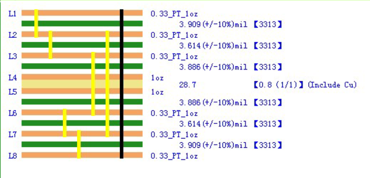
Please click here to see our HDI stackups with blind vias and buried vias.